- 您现在的位置:买卖IC网 > Sheet目录1996 > HSP45102SC-40Z (Intersil)IC OSC NCO 40MHZ 28-SOIC
5
FN2810.9
April 25, 2007
input register. At each clock, the contents of this register are
summed with the current contents of the accumulator to step to
the new phase. The phase accumulator stepping may be
inhibited by holding ENPHAC high. The phase accumulator
may be loaded with the value in the input register by asserting
LOAD, which zeroes the feedback to the phase accumulator.
The phase adder sums the encoded phase modulation bits
P0-1 and the output of the phase accumulator to offset the
phase by 0°, 90°, 180° or 270°. The two bits are encoded to
produce the phase mapping shown in Table 1. This phase
mapping is provided for direct connection to the in-phase
and quadrature data bits for QPSK modulation.
ROM Section
The ROM section generates the 12-bit sine value from the
13-bit output of the phase adder. The output format is offset
binary and ranges from 001 to FFF hexadecimal, centered
around 800 hexadecimal.
TABLE 1. PHASE MAPPING
P0-1 CODING
P1
P0
PHASE SHIFT (DEGREES)
00
0
01
90
1
0
270
1
180
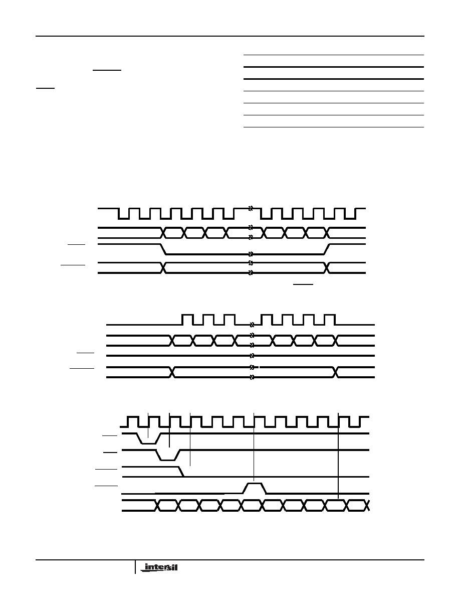
FIGURE 2A. FREQUENCY LOADING ENABLED BY SFTEN
FIGURE 2B. FREQUENCY LOADING CONTROLLED BY SCLK
FIGURE 3. I/O TIMING
SCLK
SD
SFTEN
MSB/LSB
0
1
2
63
62
61
SCLK
SD
SFTEN
MSB/LSB
0
1
2
63
62
61
CLK
LOAD
TXFR
OUT0-11
1
3
4
6
789
10
11
5
2
NEW
DATA
ENPHAC
SEL_L/M
HSP45102
发布紧急采购,3分钟左右您将得到回复。
相关PDF资料
HSP45106JC-33Z
IC OSC NCO 33MHZ 84-PLCC
HSP45116AVC-52Z
IC OSC NCO 52MHZ 160-MQFP
ICL7109EPL+
IC ADC 12BIT 3-ST 40-DIP
ICM7217AIPI
IC OSC UP/DWN CNTR 2MHZ 28-DIP
ICM7217CIPI
IC OSC UP/DWN CNTR 2MHZ 28-DIP
ICM7242IPA
IC OSC BINARY CTC 13MHZ 8-DIP
ICM7250IWE+T
IC OSC BINARY CTC 15MHZ 16SOIC
ICM7556IPD
IC OSC TIMER DUAL 500KHZ 14-DIP
相关代理商/技术参数
HSP45102SI-33
制造商:Rochester Electronics LLC 功能描述:12 BIT NUMERICALLY CONTROLLED OSCILLATOR - Bulk
HSP45102SI-3396
功能描述:可编程振荡器 12 BIT NCO 28LD SOIC,T&R,33MHZ,IND RoHS:否 制造商:IDT 封装 / 箱体:5 mm x 7 mm x 1.5 mm 频率:15.476 MHz to 866.67, 975 MHz to 1300 MHz 频率稳定性:+/- 50 PPM 电源电压:3.63 V 负载电容:10 pF 端接类型:SMD/SMT 输出格式:LVPECL 最小工作温度:- 40 C 最大工作温度:+ 85 C 尺寸:7 mm W x 5 mm L x 1.5 mm H 封装:
HSP45102SI-33Z
功能描述:可编程振荡器 W/ANNEAL 12 BIT NCO 28 33MHZ IND RoHS:否 制造商:IDT 封装 / 箱体:5 mm x 7 mm x 1.5 mm 频率:15.476 MHz to 866.67, 975 MHz to 1300 MHz 频率稳定性:+/- 50 PPM 电源电压:3.63 V 负载电容:10 pF 端接类型:SMD/SMT 输出格式:LVPECL 最小工作温度:- 40 C 最大工作温度:+ 85 C 尺寸:7 mm W x 5 mm L x 1.5 mm H 封装:
HSP45102SI-40
制造商:Rochester Electronics LLC 功能描述:- Bulk
HSP45106
制造商:INTERSIL 制造商全称:Intersil Corporation 功能描述:16-Bit Numerically Controlled Oscillator
HSP45106/883
制造商:INTERSIL 制造商全称:Intersil Corporation 功能描述:16-Bit Numerically Controlled Oscillator
HSP45106_04
制造商:INTERSIL 制造商全称:Intersil Corporation 功能描述:16-Bit Numerically Controlled Oscillator
HSP45106883
制造商:INTERSIL 制造商全称:Intersil Corporation 功能描述:16-Bit Numerically Controlled Oscillator